GPIO (Core 510i, 1100, 3100, I/O Frame)
This topic describes how to configure and control the General Purpose Input Output (GPIO) hardware interfaces in Q-SYS Designer.
The General Purpose Input Output (GPIO) interface is used to integrate Q-SYS with custom or third-party controls. The GPIO allows you to control external hardware and certain aspects of Q-SYS using external hardware. In addition, you can use the GPIO to supply an external word clock to Q-SYS for synchronization. Refer to the Core Status topic for details. The GPIO selections require an external TTL level word clock: pin 3 is signal, pin 8 is ground. When you select GPIO A-1 or GPIO B-1 as the clock source, the respective GPIO 1 Property changes to "Input used as clock source". The clock source should be connected to pin 3 of the respective GPIO connector - either GPIO A or GPIO B.
Note: Typically, Internal is used as the clock source. Only if there is a need to synchronize the Q-SYS system to an external clock would you use GPIO or AES3. You would use GPIO if the external clock signal is a word clock. You would use AES3 if the external clock signal is an AES3 signal. Often an AES3 signal without audio is used to reduce the clock jitter. This signal is called AES3 black.
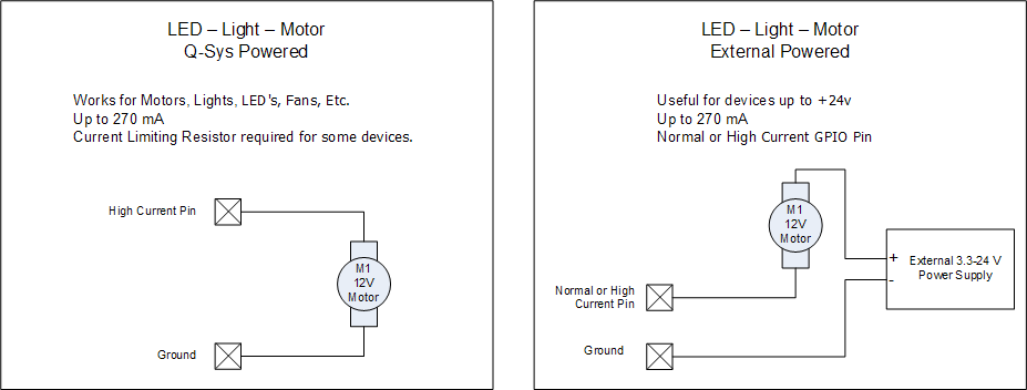
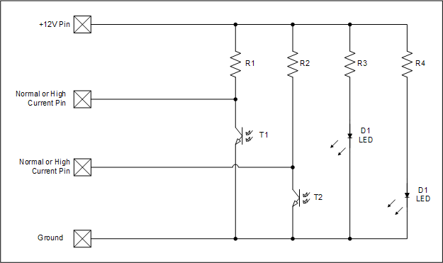
Some examples of hardware to which you can connect are: Potentiometers, buttons, switches, LED/lights, motors (including fans) relays, and temperature and humidity sensors.
The GPIO interface is physical hardware, and is represented in Q-SYS Designer by the GPIO component. There are two GPIO interfaces available in a Core, and one in an I/O Frame. The external connection to the GPIO interface is supplied via a standard DA-15 connector. A GPIO component is configured in Q-SYS Designer (GPIO component Properties) where there are eight configurable pins that represent and configure GPIO-1 through GPIO-8 in the DA-15 connector. You can configure these pins to be Inputs, Outputs, Digital, Analog, Clocks, and so on.
The GPIO is protected by self-resetting fuses.
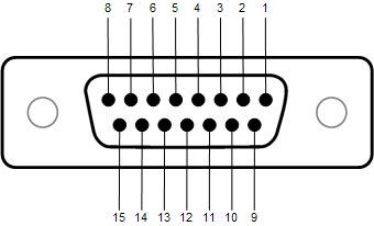
|
DB-15 Pin # |
Signal Name |
Signal Type |
Description |
|---|---|---|---|
|
1 |
RNO |
Relay Contact |
Relay Normally Open 1 |
|
2 |
RNC |
Relay Contact |
Relay Normally Closed 1 |
|
3 |
GPIO-1 |
Normal Current |
Configurable 2 |
|
4 |
GPIO-3 |
Normal Current |
Configurable |
|
5 |
Power |
Power |
+12 VDC |
|
6 |
GPIO-5 |
High Current |
Configurable |
|
7 |
GPIO-7 |
High Current |
Configurable |
|
8 |
GND |
Ground |
Ground |
|
9 |
RC |
Relay Common |
Relay Common 1 |
|
10 |
GND |
Ground |
Ground |
|
11 |
GPIO-2 |
Normal Current |
Configurable |
|
12 |
GPIO-4 |
Normal Current |
Configurable |
|
13 |
Power |
Power |
+12 VDC |
|
14 |
GPIO-6 |
High Current |
Configurable |
|
15 |
GPIO-8 |
High Current |
Configurable |
1. The GPIO Relay is controlled in a Q-SYS Design.2. When Using a Word Clock. The GPIO input impedance is much higher than what would normally be required to terminate a word clock signal. QSC recommends using a termination resistor between pin 3 and ground (pin 8 or 10). The resistor value should match the cable impedance. If the cable impedance is unknown, use 75 Ohm. Refer to the GPIO component for more information about external clocks. |
|||
| Name | Normal Current Pins | High Current Pins |
|---|---|---|
|
Maximum Input Range |
0 V to 32 V |
0 V to 32 V |
|
Analog Input Range |
0 V to 24 V |
0 V to 24 V |
|
Digital Input, Low |
0.8 V maximum |
0.8 V maximum |
|
Digital Input, High |
2.0 V minimum |
2.0 V minimum |
|
Digital Output, Low |
0.4 V maximum |
0.4 V maximum |
|
Digital Output, High |
2.4 V minimum, 3.3 V maximum |
2.4 V minimum, 3.3 V maximum |
|
Digital Output Impedance |
1 k ohm |
1 k ohm |
|
High Current Output, Low |
N / A |
0.4 V maximum |
|
High Current Output, High |
N / A |
11 V minimum, 13 V maximum |
|
High Current Output sink |
280 mA |
280 mA |
|
High Current Output source |
N / A |
280 mA |
| Specifications | ||
|---|---|---|
|
Relay Pins |
Maximum Voltage, relative to Ground |
30 V |
|
Maximum Current through Relay |
1 Amp |
|
|
Power Pins |
Output Voltage |
11 V min 13 V max |
|
Maximum Output Current |
400 mA |
|
|
All Power and High Current pins combined |
Maximum Source Current |
400 mA |
|
All GPIO Pins 1 through 8 combined |
Maximum Sink Current |
1 A using 1 GND pin 2 A using 2 GND pins |
There are four possible "Directions" you can select for the GPIO pins.
|
Property |
Value |
|---|---|
|
Unused |
The default position, and anytime the GPIO Pin is not in use |
|
Input |
Devices or signals connected to a configurable pin provide an input to the Q-SYS system. |
|
Output |
The Q-SYS hardware will be providing signals to devices connected to configurable pins. |
|
Raw |
The Raw mode is for advanced capabilities. If there is something you cannot do in the standard choices, contact QSC Support for detailed information. |
|
Property |
GPIO Pins |
Value |
|---|---|---|
|
3 |
When the Core Clock Source Property is set to GPIO A-1 or GPIO B-1, this GPIO is used only for the clock source. The GPIO selections require an external TTL level word clock: pin 3 is signal, pin 8 is ground. When you select GPIO A-1 or GPIO B-1 as the clock source, the respective GPIO 1 Property changes to "Input used as clock source". The clock source should be connected to pin 3 of the respective GPIO connector - either GPIO A or GPIO B. Note: Typically, Internal is used as the clock source. Only if there is a need to synchronize the Q-SYS system to an external clock would you use GPIO or AES3. You would use GPIO if the external clock signal is a word clock. You would use AES3 if the external clock signal is an AES3 signal. Often an AES3 signal without audio is used to reduce the clock jitter. This signal is called AES3 black. |
|
|
Digital |
1 to 8 |
Digital zero = 0 Digital one = 3.3 |
|
Potentiometer |
1 to 8 |
Allows a potentiometer to be connected to the GPIO pin, the position of which is represented by the control in the GPIO Control Panel. The value or range is 0 to 1. |
|
Analog |
1 to 8 |
Input 0 to 24 V, Low Z 12-bit Resolution |
|
Contact Closure |
1 to 8 |
Allows a button, switch, or other binary device to be connected to the GPIO Relay contact. |
|
WCP-1 |
1 to 8 |
Interfaces with QSC's Wall Control Plate, version 1. Refer to the WCP Installation Guide for more information. |
|
WCP-2 (3 pins) |
1-3 and/or 5-7 |
Selectable on GPIO pins 1 and 5 only. Interfaces with QSC's Wall Control Plate, version 2. Requires three configurable pins. Refer to the WCP Installation Guide for more information. |
|
Optical Rotary Encoder |
1-2, 3-4, 5-6, or 7-8 |
Allows an Optical Rotary Encoder to be connected to two configurable pins. |
|
Mechanical Rotary Encoder |
1-2, 3-4, 5-6, or 7-8 |
Allows a Mechanical Rotary Encoder to be connected to two configurable pins. |
|
Property |
GPIO Pins |
Value |
|---|---|---|
|
Digital Output |
1 to 8 |
Digital zero = 0 Digital one = 1 |
|
Pulse Width Modulated (PWM) Output Good for operating a Fan or a DC motor that will likely require 12 V High Drive, High Current. |
1 to 8 |
Pulse Width is set in the Control Panel 0 - 100% Pulse Frequency is set in the Control Panel 50 to 50,000 Hz |
|
Inverted Pulse Width Modulated (PWM) Output If this pin is used in conjunction with the non-inverted PWM, linking the PWM Duty Control Pins together will produce opposite but equal signals since they must use the same frequency. |
1 to 8 |
Pulse Width is set in the Control Panel 0 - 100% Pulse Frequency is set in the Control Panel 50 to 50,000 Hz |
|
No Clock output available on these pins |
1 and 5 |
N / A |
|
Sample Clock |
2 and 6 |
System Frequency 48 kHz |
|
Vector Clock |
3 and 7 |
3 kHz 6 kHz |
|
Frame Clock Mainly intended for software debug. |
4 and 8 |
Programmable - 30 Hz to 120 Hz |
|
Property |
Value |
|---|---|
|
GPIO Pins 1 - 4 |
3.3 V TTL Open Collector High Current |
|
GPIO Pins 5 - 8 |
3.3 V TTL 12 V Push-Pull High Current 12 V High-Drive High Current Open Collector High Current |
The Raw mode is for advanced capabilities. If there is something you cannot do in the standard choices, contact QSC Support for detailed information. Note that when you select Raw as the direction, there are two instances of that pin on the GPIO component; one input, and one output.
The Controls are displayed in GPIO Pin number order, 1 through 8, from left to right in the Control Panel with the related DA-15 pin number listed. The DA-15 pin / GPIO pin number relationship can change based on the controls assigned to the GPIO pins.
General
|
Control |
Function |
Default / Range |
|---|---|---|
|
Relay |
The function of the Relay button is to open and close the contacts of the relay on the GPIO Interface. RNO 1 (Relay Normally Open on DA-15 Pin 1) RNC 2 (Relay Normally Closed on DA-15 Pin 2) RC 9 (Relay Common on DA-15 Pin 9) |
Off / On |
|
Digital In (Indicator) |
This LED lights when there is a Digital input of 1 (3.3 V TTL) present. |
Off / On |
|
Analog In (VDC) |
This is a read-only knob that displays the DC voltage applied to the GPIO pin. |
Default = 0 Range = 0 to 12 |
|
Digital Out |
This toggle button supplies a 0 in the Off position and a 1 in the On position. |
Off / On |
|
PWM Duty (Percentage) |
Sets the percentage of a period when the pulse is positive. |
Default = 0 Range = 0 to 100 |
|
PWM Frequency (Hz) |
Sets the period time. (1 / frequency) Affects all PWM outputs |
Default = 50 Range = 5 to 50,000 |
The GPIO pins display as control pins on the GPIO component and are always present except when "Unused" is selected for a pin's Direction. The GPIO pins are not used to change controls in the Control Panel. Some of the Direction/Type combinations provide Control Pins you can use to change the Controls within the Control Panel.
The Relay Out Control Pin is always available.
|
Pin Name |
Value |
String |
Position |
Pins Available |
|---|---|---|---|---|
|
Relay Out |
0 1.00 |
false (normal) true (activated) |
0 1.00 |
Input / Output |
The Pin Name reflects the Input Type you select for a given GPIO pin. Indented below each GPIO Type are any Control Pins that may be available for that Type.
|
Pin Name |
Value |
String |
Position |
Pins Available |
|---|---|---|---|---|
|
Digital Input |
0 1 |
false true |
0 1 |
Output |
|
Contact Closure |
0 1 |
false true |
0 1 |
Output |
|
Potentiometer (10k Ohm, 12 V) and Potentiometer (2-wire) |
0 to 1 |
N / A |
0 to 1.00 |
Output |
|
Calibrate Maximum |
|
|
|
|
|
Calibrate Minimum |
|
|
|
|
|
Maximum Position |
|
|
|
|
|
Minimum Position |
|
|
|
|
|
Analog Input |
0 to 24.00 |
0.00 V to 24.0 V |
0 to 1.00 |
Output |
|
WCP-1 |
0.00 1.00 2.00 3.00 4.00 5.00 6.00 7.00 8.00 9.00 10.00 |
0 1 2 3 4 5 6 7 8 9 10 |
0 .100 .200 .300 .400 .500 .600 .700 .800 .900 1.00 |
Output |
|
WCP-2 |
1.00 2.00 3.00 4.00 5.00 6.00 |
1 2 3 4 5 6 |
0 .200 .400 .600 .800 1.00 |
Output |
|
Rotary Encoder (Mechanical or Optical) |
0 to 1.00 |
N / A |
0 to 1.00 |
Input / Output |
|
Rotary Encoder Resolution |
4 to 4096 |
4 to 4096 |
0 to 1.00 |
Input / Output |
|
Rotary Encoder Reverse |
0 1.00 |
normal invert |
0 to 1.00 |
Input / Output |
The Pin Name reflects the Output Type that must be selected for a particular Control Pin to be available.
|
Pin Name |
Value |
String |
Position |
Pins Available |
|---|---|---|---|---|
|
Digital Output 1 |
0 1 |
false true |
0 1 |
Input / Output |
|
PWM Output |
0 to 100 |
— |
0 to 1.00 |
Input / Output |
|
PWM Duty |
0 to 100 |
0% to 100% |
0 to 1.00 |
Input/Output |
|
PWM Invert |
0 1.00 |
normal inverted |
0 to 1.00 |
Input / Output |
|
PWM Frequency |
5 to 50,000 |
5.00Hz to 50.0kHz |
0 to 1.00 |
Input / Output |
|
Inverted PWM Output |
0 to 100 |
— |
0 to 1.00 |
Input / Output |
|
PWM Duty |
0 to 100 |
0% to 100% |
0 to 1.00 |
Input/Output |
|
PWM Invert |
0 1.00 |
normal inverted |
0 to 1.00 |
Input / Output |
1. When Digital Output is selected, the Control Pin for the "Digital Out" button in the Control Panel displays as an input to the selected GPIO pin. It is not shown in the Control Pins list as other "Control Pins". |
||||
Button or Potentiometer

LED - Light - Motor
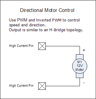
Directional Motor
Rotary Encoder
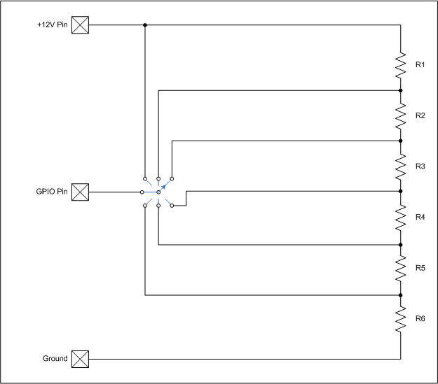
Rotary Switch
All resistors should have the same value. The total resistance should be about 10K Ohms. The individual resistor value should be 10,000 divided by the number of resistors. The schematic is an example only, and could easily be modified to have more switch positions or use multiple momentary buttons instead of a rotary switch.
Q-SYS device GPIO output states are undefined during boot-up and design redeploy. In the following table, "While On" and "While Off" indicate the button setting as defined in the running design file. During a reboot or redeploy, the setting may toggle depending on the GPIO type before returning to the defined setting after the design starts running.
Bold text indicates a temporary GPIO setting during boot-up and redeploy.
|
GPIO Type |
While On |
While Off |
|---|---|---|
|
Digital Output |
Toggles to Off |
Stays Off |
|
Open Collector |
Toggles to Off |
Stays Off |
|
Raw |
Stays On |
Toggles to On |
|
GPIO Type |
While On |
While Off |
|---|---|---|
|
Digital Output |
Stays On |
Toggles to On |
|
Open Collector |
Toggles to Off |
Stays Off |
|
Raw |
Stays On |
Toggles to On |
|
GPIO Type |
While On |
While Off |
|---|---|---|
|
Digital Output |
Toggles to Off |
Stays Off |
|
Open Collector |
Toggles to Off |
Stays Off |
|
Raw |
Stays On |
Toggles to On |
|
GPIO Type |
While On |
While Off |
|---|---|---|
|
Digital Output |
Toggles to Off |
Stays Off |
|
Open Collector |
Stays On |
Toggles to On |
|
Raw |
Stays On |
Toggles to On |
